The ongoing miniaturization and increased density of electronics lead to more frequent occurrences of various defects both during the manufacturing of printed circuit boards and the assembly process. Therefore, precise inspection of the finished product becomes crucial.
Modern automatic optical inspection (AOI) devices guarantee fast and accurate checking of solder joint quality. However, the limitations of this method become evident when inspecting connections under component enclosures, such as in BGA, CSP, or flip chip structures. In such cases, X-ray inspection becomes indispensable.
What is X-ray inspection of electronics?
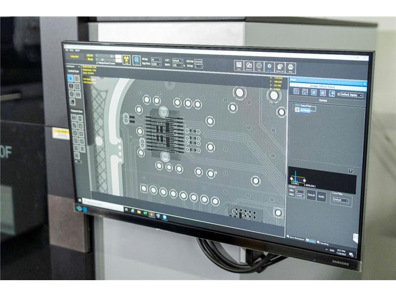
X-ray inspection of electronics is a process that uses X-ray radiation to examine the internal structure of electronic devices. This allows the inspection of the interior of an object without dismantling it. This is invaluable, especially in the context of modern electronics where miniaturization and increased component density can make defect detection challenging.
Automatic X-ray inspection enables the quick and precise detection of various defects such as cracks, improper solder joints, or the presence of foreign objects. This technology has found wide application in the electronics industry, contributing to reduced production time, improved quality, and increased efficiency of production processes.
Advantages of X-ray inspection
The main advantage is undoubtedly the ability to quickly detect errors that are invisible to other techniques. The non-invasive nature of this method allows for the examination of complex systems without damaging them. This enables early detection and correction of errors, leading to higher final product quality and cost savings.
Compared to traditional inspection methods, which often require device disassembly or evaluation of only external components, X-ray technology allows for a thorough assessment of the device’s interior. This means that even the most hidden defects can be detected and repaired before delivering the product to the end customer.
Using X-ray technology to detect defects
X-ray inspection allows us to examine complex components, including BGA, CSP, or LEDs. Quality control of solder joints for miniature components like BGA and CSP becomes impractical without using X-rays due to the dense arrangement of pins under the enclosure, making traditional observation difficult.
The assembly of components with leads hidden under the enclosure must be done precisely, especially on boards with microvias. Incorrect choice of paste or soldering profile can lead to voids. Therefore, frequent inspection of connections using X-rays is crucial to minimize the risk of defects. Conducting X-ray inspections must consider that soldering quality depends on many aspects. Defects in solder joints can be visible both immediately after assembly and after prolonged product use. Another issue identifiable through X-ray technology is the so-called “cold solder” in BGA and CSP components.

This defect occurs when the paste and solder do not fully coalesce during the soldering process. Without X-ray inspection, it would be difficult to notice this defect as the connection may initially be electrically functional.
Although electronic boards also contain less complex components besides BGA and CSP, like resistors or capacitors, their soldering quality control also requires advanced X-ray analysis. This examination can reveal various defects, including voids or component misalignment. Fortunately, such defects can often be corrected, and after additional inspection, the product is ready for further use by the customer.
Accurately assessing the quality of a printed circuit board is a significant challenge, especially if we do not want to damage the examined element. Traditional observation methods, even with a microscope, do not provide results as accurate as X-ray examination, which allows for a precise assessment of track quality and comparison with customer expectations.
Development of X-ray inspection technology in electronics
Modern X-ray inspection systems often utilize advanced software that enables in-depth image analysis, automatic defect detection, and classification. These solutions contribute to even greater efficiency and accuracy of inspections. Moreover, X-ray inspection is flexible and can be applied to examine various products, from simple components to more advanced systems.
The development of this technology has brought numerous innovations, such as higher image resolution, faster scanning, and advanced analytical software. As a result, X-ray inspection has found broad applications in the industry, contributing to reduced production time, improved quality, and increased efficiency of production processes.


X-ray inspection services by RENEX Group
RENEX Group offers two key approaches in X-ray inspection. One involves clients sending samples to our Technological Training Center, providing problem details. After X-ray analysis, the results, compliant with IPC standards, are emailed to the client, typically within 1-2 business days. The other option is purchasing X-ray equipment, allowing immediate control with the release of the first product in a series, enabling quick corrections before continuing production.
Advanced users will also appreciate the ability to take images of work directly through the ZIP microscope. Simply connect it to a computer and use the built-in Windows OS Camera application. The TAGARNO ZIP offers high quality and precision, combined with practicality, making it ideal for professional electronics repair, providing an excellent value for money.
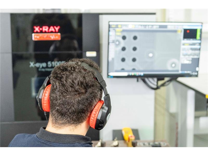
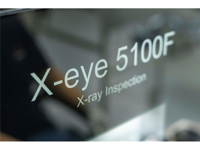
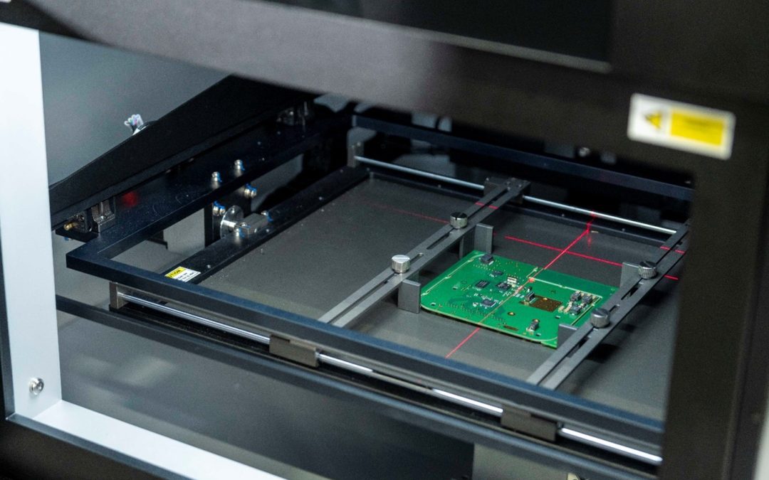
RENEX has equipment for purchase that can be integrated into the production process. An example is the SEC X-RAY 5100F device, whose installation has been approved by the State Atomic Agency. The process is simplified for the client – after purchase, the device can be integrated into production, with formalities handled by the distributor. This is crucial due to the necessity of training personnel involved in the installation. Each installation is reported to the PAA by our group to ensure safety. X-ray inspections are used to identify component defects and quality control, applicable in various sectors such as automotive or construction. RENEX offers various services in this area, including the possibility of purchasing testing equipment and sending samples to our Center.
RENEX Group does not limit itself to X-ray inspections. It provides a wide range of training and consultations related to production processes. Clients can benefit from the TECHNOLOGICAL TRAINING CENTER and DEMOROOM, where modern solutions from the electronics and robotics industry are presented. Supported by our experts, clients can choose the best solutions for themselves. RENEX guarantees comprehensive support at every stage of order fulfillment. The company’s advisors maintain constant contact with clients, monitoring their needs and supporting subsequent projects. With knowledge and experience, the company can meet even the most advanced expectations, striving for full customer satisfaction. More information about contacting a Technical Sales Advisor can be found at RENEX website
